

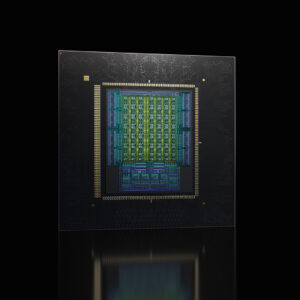

Keysight Technologies and WIN Semiconductors have collaborated on a joint MMIC design workflow aimed at reducing fabrication risks for gallium nitride (GaN) MMIC developers. The workflow brings on-chip multi-domain simulation, layout verification, and off-chip evaluation board design into a unified environment. It combines WIN Semiconductors’ GaN Process Design Kit, including process models and layout rules, with Keysight’s Advanced Design System and RF Circuit Simulation Professional.
The approach aims to automate simulation, optimization, and verification before fabrication while allowing engineers to evaluate chip and board-level performance together. The workflow is intended to support applications including mobile infrastructure, Wi-Fi access points, satellite payloads, and defense radar systems.
Image generated by: Gemini