

Siemens and TSMC have expanded their collaboration to advance AI-enabled semiconductor design workflows and support next-generation process technologies. The partnership focuses on integrating Siemens’ Fuse EDA AI system across electronic design automation (EDA) workflows, including automated design rule check (DRC) correction, physical verification, and digital implementation. Siemens also announced certifications for multiple EDA tools supporting TSMC’s N3A, N3C, N2P, A16, and A14 process nodes.
In addition, the companies are extending collaboration on 3D IC design, thermal analysis, silicon photonics, and TSMC’s 3DFabric technologies. The initiative aims to address growing semiconductor design complexity associated with AI, high-performance computing, and advanced packaging architectures.
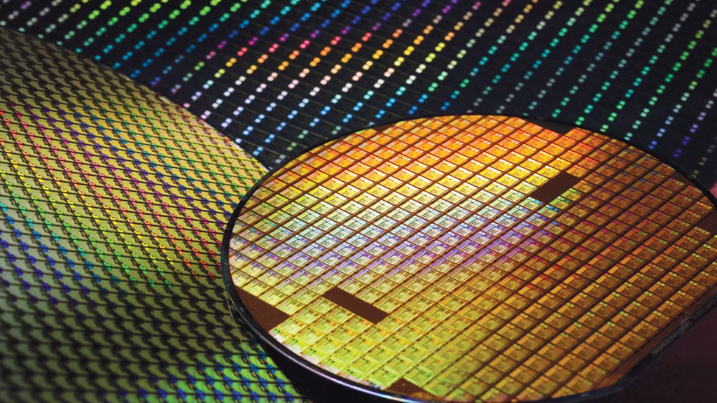
Image courtesy: TSMC